CORE TECHNOLOGY

One connected power semiconductor technology, from device to system

Dicio designs high-voltage power semiconductor devices and module packages together. Chip, package and design-in are connected as one platform to optimise conduction loss, switching loss, heat and system reliability.

600–4500 VSi IGBT · SiC Platform
1.9 mΩ·cm²1200 V SiC MOSFET Rsp · Gen 2
66 / 66Superior at every measured PCS point
DEVICESiC MOSFET · Si IGBT
MODULEHybrid · Full SiC · Packaging
APPLICATIONCustomer System · Design-in
ONE TECHNOLOGY PLATFORM

01 · DEVICE TECHNOLOGY

SiC MOSFET Core Design

Low on-resistance, fast switching, stable operation at 175 ℃

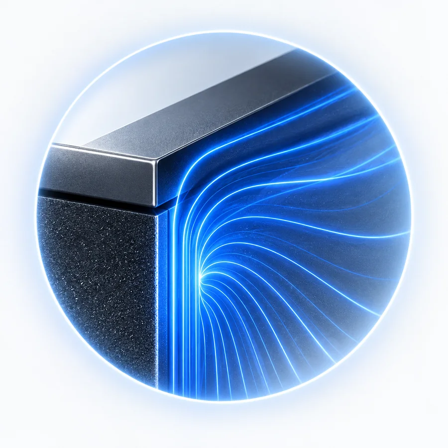
Dicio directly designs the cell pitch, JFET, channel, gate oxide and gate structure that determine SiC MOSFET performance.

600–3300 VSiC Platform
1.9 mΩ·cm²1200 V Gen 2
175 ℃Operating Temperature
SiC MOSFET vertical cell cross-section

RDS(on) ↔ SWITCHING LOSS TRADE-OFF

Switching OptimizedConduction OptimizedRDS(on) →Switching Loss →DICIO Target
DESIGN DIRECTION FOR HIGH LOAD
RDS(on) ↓Lower conduction loss
Chip Area ↑Higher switching charge
High-current operationEfficiency optimisation

02 · DEVICE TECHNOLOGY

High-Voltage SiC MOSFET &SiC Schottky Diode

High-voltage SiC design changes beyond 1200 V

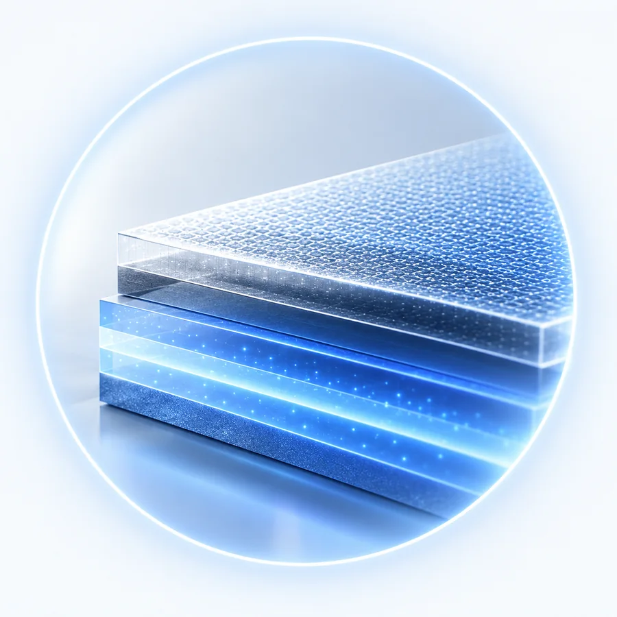
Beyond 1200 V, drift-layer and electric-field control become critical. Dicio optimises Epi, edge termination and cells for each voltage class, while co-designing SiC Schottky diode VF, leakage and surge characteristics to balance on-resistance and blocking voltage.

EPI / DRIFT high-voltage SiC design

EPI / DRIFT

Thickness · Doping

Thickness and doping are designed for each voltage class to balance high-voltage blocking and on-resistance.

EDGE TERMINATION high-voltage SiC design

EDGE TERMINATION

Electric Field Control

Edge electric fields are distributed effectively to control blocking-voltage margin and leakage.
SCHOTTKY / JBS high-voltage SiC design

SCHOTTKY / JBS

VF · Leakage · Surge Reverse Recovery ≈ 0

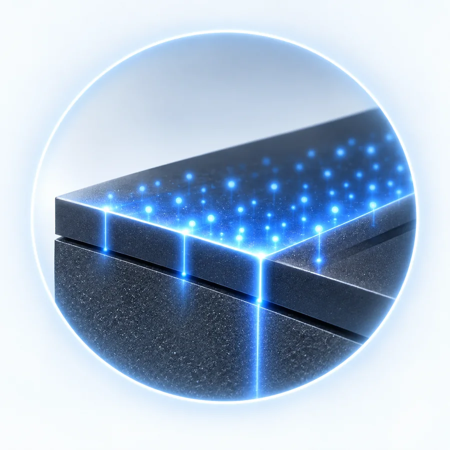
The Schottky barrier and P+ structure are optimised for low forward voltage, controlled leakage, surge capability and near-zero reverse recovery.

DICIOHigh-Voltage SiC Platform
1200 VRsp 1.9 mΩ·cm²
1700 VKorea's First
2000 V1500 V DC · 2-Level
2300 V1500 V DC · 2-Level
3300 VGridFRAME™ 2 MMC · SST · MV Drive

03 · DEVICE TECHNOLOGY

High-VoltageSi IGBT Design

We design total system loss, not a single parameter.

VCE(sat) and Eoff have a trade-off relationship. Dicio minimises total system loss by balancing conduction and switching losses for the target switching frequency and load profile.
VCE(sat) – Eoff TRADE-OFF

1.41.61.82.02.22.402468101214VCE(sat) [V]Eoff [mJ]
Low Conduction Loss CellFor high-load operation(1.6 V, 8.6 mJ)
Low Switching Loss CellFor high switching frequency(2.2 V, 4.8 mJ)

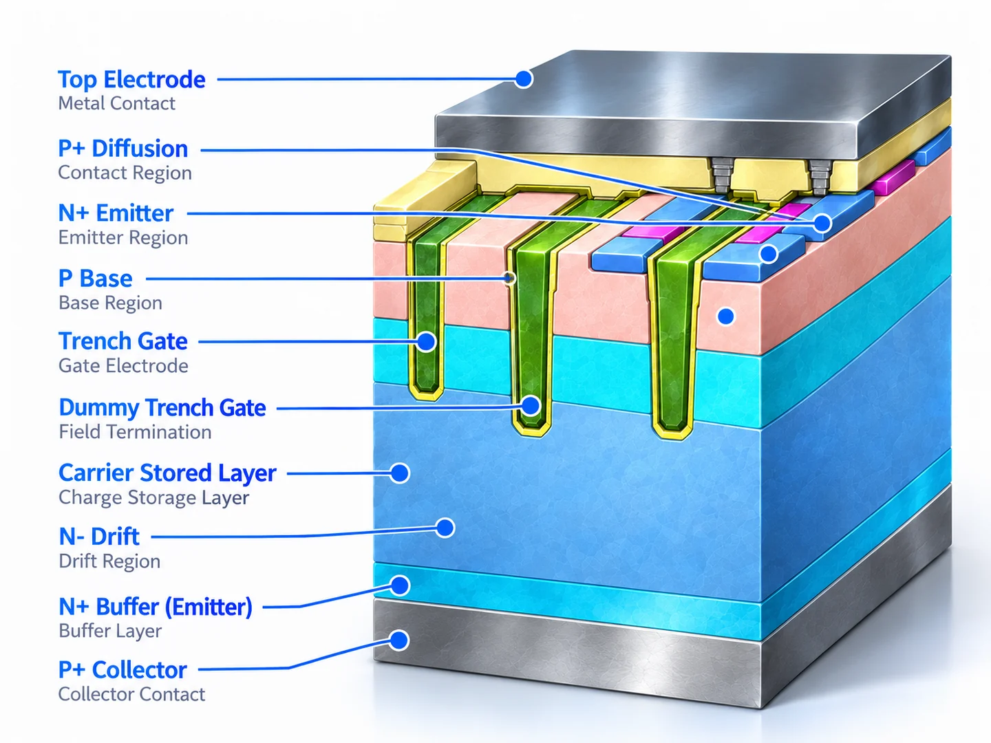
FIELD-STOP TRENCH-GATEVERTICAL STRUCTURE

Field-Stop Trench-Gate Si IGBT vertical structure
DICIOSi IGBT Platform
600 VLow Voltage
1200 VMainstream
1700 VHigh Voltage
2300 VExtended HV
3300 VMV Class
4500 VHighest Class

04 · MODULE TECHNOLOGY

Hybrid & Full SiC Module Design

Choose the optimum balance of efficiency and economy within the same footprint.

Dicio extends one footprint platform from Si IGBT to Hybrid and Full SiC, placing the right device characteristics at each switching position in the converter.
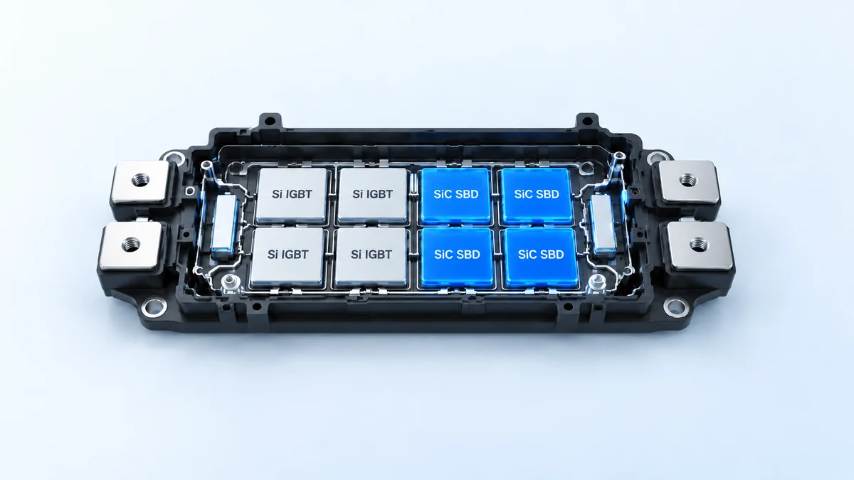
◇01 SAME FOOTPRINTSame housing · same terminals · same cooling. Only the chip technology changes.
▦02 HYBRID / FULL SiCSi IGBT + SiC SBD balances economy and performance, with a path to Full SiC.
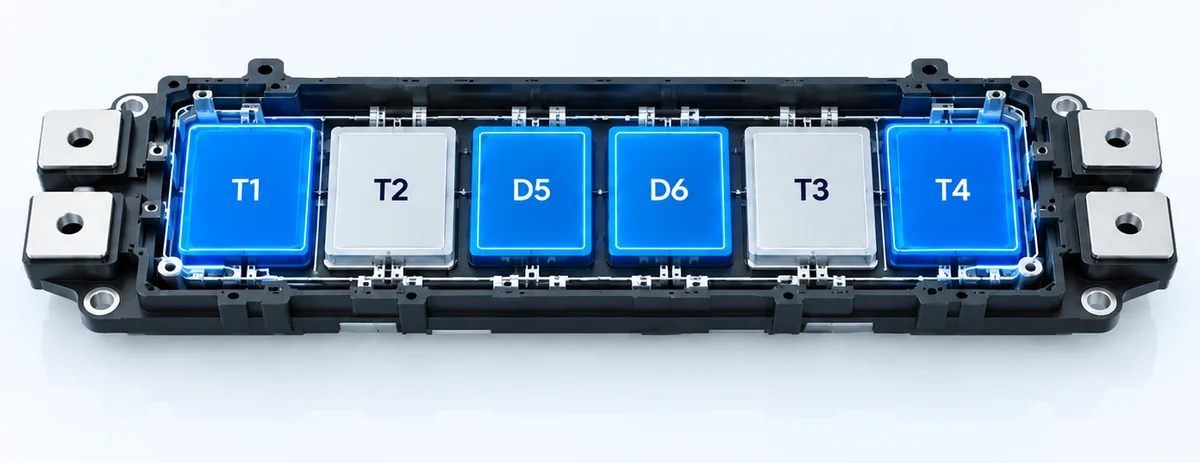
≋03 POSITION OPTIMIZATIONDevice characteristics are assigned by switching position to optimise system losses.
DICIOFull SiC Module Platform1200–3300 V2-Level / 3-Level NPC · Same Footprint Family

SAME FOOTPRINT PLATFORM

본 이미지는 실제 제품이 아닌 개념도입니다.Hybrid chip configuration in the same module housing
HYBRID
  • Si IGBT + SiC SBD
  • Reverse Recovery ≈ 0
  • Turn-on Loss ↓
  • Drop-in Upgrade

3-LEVEL NPC · POSITION OPTIMIZATION

본 이미지는 실제 제품이 아닌 개념도입니다.NPC module concept showing T1, T2, D5, D6, T3 and T4 positions
T1 / T4 · OUTER SWITCH

Low Switching Loss IGBT · PWM Frequency Dominant

DICIO · Full SiC Module Platform1200–3300 V2-Level / 3-Level NPC · Same Footprint Family

05 · MODULE TECHNOLOGY

Low-Inductance Packaging &Thermal Path

Stabilise fast switching, then remove generated heat quickly.

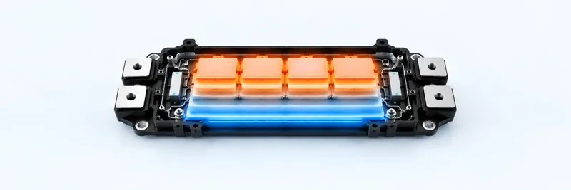
Dicio designs the DC+ / DC− current path, parallel chip layout and Gate·Kelvin Return together with the chip — through DBC, baseplate, joining materials and the cooling path.
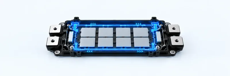
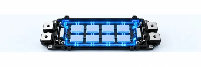
≤ 10 nHLs,CE Switch Parasitic Inductance
0.017 K/WRth(j-c)
57,710Power Cycling ΔTj 100 K

ELECTRICAL PATH

Low-inductance commutation loopSymmetric parallel chip current sharing

LOW INDUCTANCE

  • DC+ / DC− Close Routing
  • Short Commutation Loop
  • Symmetric Current Sharing
  • Gate / Kelvin Separation
Ls,CE ≤ 10 nHΔV = Lσ × di/dt

THERMAL PATH

Thermal stack from chip to coolant
  • SiC / Si CHIP
  • Ag Sintering / Solder
  • DBC (AlN · Si₃N₄ · Al₂O₃)
  • Baseplate (Cu / AlSiC)
  • TIM
  • Heatsink / Coolant

Designing the full thermal path from chip to cooling secures low thermal resistance and high durability.

06 · APPLICATION TECHNOLOGY

Application-Optimized Design

We do not fit the system to the product. We design the product for the system.

We start from real operating conditions and co-design devices, modules and validation to deliver the optimal solution for your application, achieving higher performance, greater reliability and faster time to market.
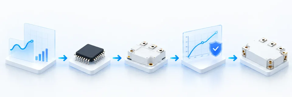
Process from customer operating conditions through device and module design and system validation to a DICIO product
2 WeeksOperating Conditions → Product Proposal
66 / 66Customer PCS Operating Points
Up to 43%System Loss Reduction

CUSTOMER CONDITIONS

CUSTOMER CONDITIONS

We first define the real operating conditions of the customer system.

  • Topology
  • DC-Link Voltage
  • Load Profile
  • Switching Frequency
  • Cooling
  • Lifetime Target

Design starts by defining the customer system inputs, not by selecting a catalogue part.

PROVEN IN SYSTEM

Technology is proven in the customer's system.

66 / 66

Customer ESS PCS · superior efficiency at every operating point

Up to 43%

System conversion loss reduction versus existing module

1700 V / 1400 A

Standard footprint high-current hybrid module

Where is the optimum point in your system?

Share your DC-link voltage, output, switching frequency, cooling conditions and lifetime target. Dicio will propose the optimum power semiconductor solution from device to module.