Technology

Research

Building the next generation of power semiconductors first

RESEARCH & DEVELOPMENT

Building the next generation of power semiconductors first

DICIO's advanced research addresses technologies one generation ahead of the production roadmap, beginning at the device-design stage. Our current focus is a 3.3 kV Full SiC-based 800 V DC solid-state transformer and a 1200 V SiC SenseFET with current sensing integrated directly on-chip.

3.3 kV / 750 AFull SiC Module Target
22.9 kV → 800 V DC1 MW-class SST
1000 : 1SenseFET Current Sensing Ratio

RESEARCH 01

For next-generation AI data centers

800 V DC Solid-State Transformer (SST)

From 22.9 kV to
800 V DC, with half
the conversion stages

We are developing an SST system and Power Cell that connect a 22.9 kV distribution grid directly to 800 V DC, together with its key switch: the 3.3 kV / 750 A Full SiC Half-Bridge Module, GridFRAME™ 2.

CONVENTIONAL AC DISTRIBUTION

22.9 kV MV AC
Low Frequency Transformer
Low-Voltage Switchgear / UPS
PDU / Server PSU
IT Rack
4-Step ConversionSystem Efficiency 93.6%


SST-BASED 800 V DC

22.9 kV MV AC
Solid-State Transformer MV AC → 800 V DC
800 V DC Bus
Server DC/DC
IT Rack
2-Step ConversionSystem Efficiency 97.0%
+3.4 %p

Target system efficiency improvement

93.6% → 97.0%

30–50%

Target footprint reduction

4 → 2

Power conversion stages

SST CORE TECHNOLOGY
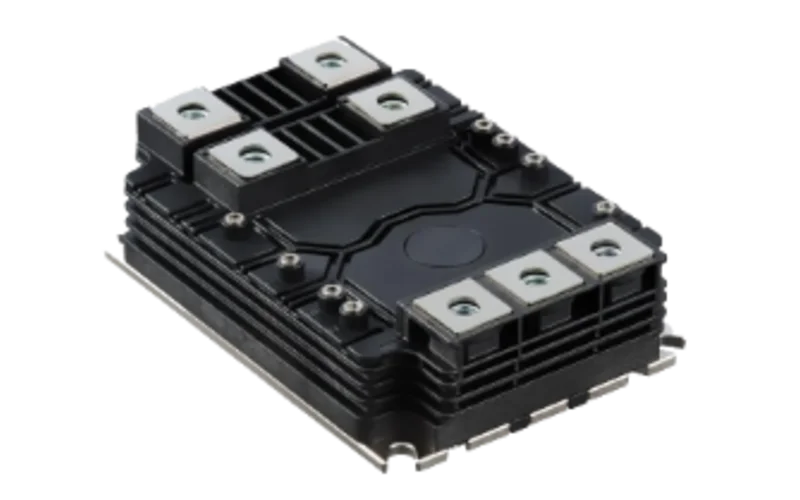
The core of the SST is a 3.3 kV Full SiC Power Module

GridFRAME™ 2

3.3 kV / 750 A Full SiC Half-Bridge

A high-voltage SiC power-module platform for the CHB and the DAB primary stage of an SST Power Cell.

3.3 kV SiC MOSFET Device

  • 3.3 kV-class Cell Structure
  • High-voltage termination electric-field design
  • Gate Oxide Reliability
  • Temperature-dependent RDS(on) and switching optimization
  • Joint foundry and wafer development

GridFRAME™ 2 Package

  • DBC Layout
  • Busbar Parasitic Inductance Simulation
  • Ls,CE ≤ 10 nH Target
  • AlN Substrate
  • AlSiC Baseplate
  • 6 kV Isolation / Partial Discharge Design
  • Cu Metallization / Ag Sintering

Reliability & Evaluation

  • Static Characteristics
  • Double Pulse Test
  • Eon / Eoff
  • dv/dt · di/dt
  • Dielectric Withstand
  • Partial Discharge
  • Short-Circuit Test
  • Power / Thermal Cycling
  • Lifetime prediction based on AI Data Center Mission Profile

Target Specification

TopologyHalf-Bridge · Full SiC · NTC
Voltage / Current3300 V / 750 A
Peak Current1500 A
RDS(on)≤ 2.5 mΩ
Eon / EoffAt or below benchmark
Isolation6.0 kV rms
Parasitic Inductance≤ 10 nH
Thermal Resistance≤ 33 K/kW
Operating Temperature−40 ~ 175°C
Footprint140 × 100 × 40 mm

SST DEVELOPMENT ROADMAP

From device to
1 MW grid-connected system

01

PHASE 01

MODULE

DICIO

2026 · Current

  • 3.3 kV SiC MOSFET
  • GridFRAME™ 2 Module
  • Prototype
  • Evaluation & Reliability System
02

PHASE 02

POWER CELL

Partner Joint Development

250 kW PoC

  • CHB + DAB Power Cell
  • Driver / Protection
  • Cell Balancing
  • MFT Joint Design
  • Control Joint Design
03

PHASE 03

SYSTEM

Partner Joint Development
  • 500 kW System
  • 1 MW System
  • 22.9 kV Grid Demonstration
04

PHASE 04

STANDARD & SCALE

Partner Joint Development
  • Purchase Specification
  • Type-Test Criteria
  • KEPCO LVDC Integration
  • Global Supply Chain
  • Standardization

RESEARCH 02

1200 V SiC SenseFET

Current sensing, integrated into the chip

DICIO's proprietary SiC device integrates a separate Sense MOSFET inside the Main MOSFET to measure 1/N of the main current directly. To address the short withstand time of SiC MOSFETs, it targets short-circuit detection and turn-off within approximately 1 µs.

SENSEFET CONCEPT

Main CellN parallel cells
Sense Cell1 Cell
Gate / Drain Shared
Source Separated
SENSING RATION = 1000 : 1

Main Current 10 A Sense Current 10 mA

SHORT-CIRCUIT PROTECTION FLOW

01
I_main surge
02
I_sense rise
03
V_sense ≥ V_ref
04
Protection IC activation
05
Gate Soft Turn-Off
06
Main Current interruption
TARGET≈ 1 µs

SENSEFET DESIGN TARGET

Faster protection, smaller systems

DESAT

Detection SpeedSlow
Main-path LossNone
External BOMRequired
Noise ImmunityAffected by dv/dt

Shunt

Detection SpeedMedium
Main-path LossPresent
External BOMRequired
Noise ImmunityParasitic inductance

External Sensor

Detection SpeedMedium
Main-path LossNone
External BOMLarge
Noise ImmunityBandwidth impact

DICIO SenseFET

Detection SpeedFastest
Main-path LossNone
External BOMMinimized
Noise ImmunityHigh
1200 V

Voltage Class

60 mΩ

RDS(on), typ.

1000 : 1

Current Sensing Ratio

> 5 V

Sense–Main Isolation

≤ 10%

25 → 175°C Sensing Ratio Variation

≈ 1 µs

Short-Circuit Detection & Turn-Off Target

TARGET APPLICATION

Compact SiC IPM / SPMIndustrial Motor Drive

DEVELOPMENT SCHEDULE

2026Device Design
2027 Q1Prototype
2027 Q2ES
2027 Q4QS

OPEN RESEARCH

From joint research to the next production technology

RESEARCH 01

800 V DC SST

3.3 kV Full SiC Device
GridFRAME™ 2
250 kW Power Cell
500 kW
1 MW Grid Demonstration

RESEARCH 02

1200 V SiC SenseFET

Device Design
Current Sensing
Short-Circuit Protection
Compact SiC IPM

JOINT RESEARCH AREAS

High-Voltage SiC DevicePower ModuleSST Power CellMedium-Frequency TransformerProtection & ControlIndustrial SiC IPMSystem Demonstration

Develop the next generation of power semiconductors
with us

DICIO develops devices and modules directly, and validates Power Cells, systems and application technologies together with partners.